
Shenyang Expert Workstation Construction Enters High-quality Development Stage
Shenyang Expert Workstation Construction Enters High-quality Development Stage
——Case Study on Shenyang StarLight Advanced Ceramics Co., Ltd.
I. Policy-driven Innovation Platform Development
In alignment with the "Three-Year Action Plan for Comprehensive Revitalization and Breakthrough of Liaoning Province (2023-2025)", Shenyang Association for Science and Technology officially issued the "Implementation Plan for Promoting the Construction of Academician (Expert) Workstations and Society Service Stations in Shenyang" (SYKX No.45, 2023) in December 2023. The plan outlines the establishment of 50 industry-leading expert workstations during the 14th Five-Year Plan period, with prioritized support for strategic emerging industries including advanced equipment manufacturing, new materials like silicon carbide, and semiconductors. According to third-party evaluation data, by October 2024, the city has established 8 academician workstations and 32 expert workstations, attracting 217 high-level experts and facilitating 89 industry-university-research collaboration projects.
Against this policy backdrop, Shenyang StarLight Advanced Ceramics Co., Ltd, a leading enterprise in advanced ceramic silicon carbide materials, proactively applied for the 2024 Expert Workstation program. After undergoing a rigorous six-month evaluation process including:
Qualification review: Verification of R&D intensity (5.2% average in recent three years) and patent portfolio (23 authorized invention patents)
Expert evaluation: Technical feasibility assessment by a 7-member panel led by Prof. Pan Wei from Tsinghua University
Party committee deliberation: 3 special sessions by SYAST leadership
Public disclosure: 15-working-day on municipal portal with 12 valid feedbacks addressed
The company was officially accredited as a pilot unit in November 2024.
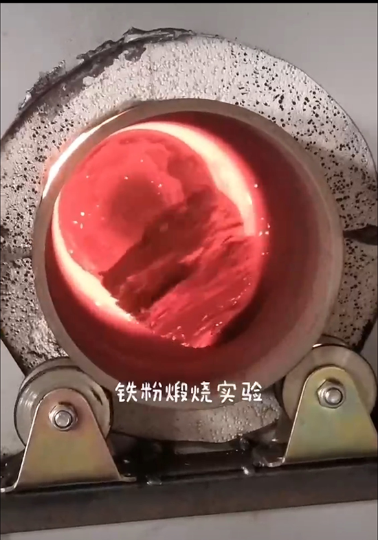
II. Technological Breakthrough Focus
The workstation concentrates on developing specialty ceramics for wafer fabrication—the core segment of semiconductor manufacturing. Statistics show the global silicon carbide ceramics market for semiconductors is projected to grow from 1.87 billionin 2023 to 5.43 billion by 2030 at a 16.4% CAGR. However, domestic import dependency for 300mm silicon carbide wafer boats remains alarmingly high at 92%, posing critical supply chain risks.
Technical roadmap includes:
Large-scale boat manufacturing: Breakthrough in CIP forming process for 450mm-diameter components with 3±0.1mm wall thickness
High-purity material development: Achieve total metallic impurities <50ppm in silicon carbide powder
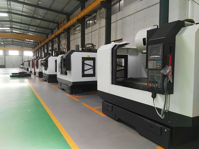
Precision machining: Establish dedicated parameter database for 5-axis CNC systems
Quality assurance: Build full-scale automated inspection platform compliant with SEMI F47
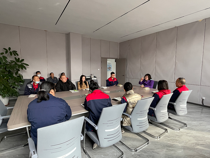
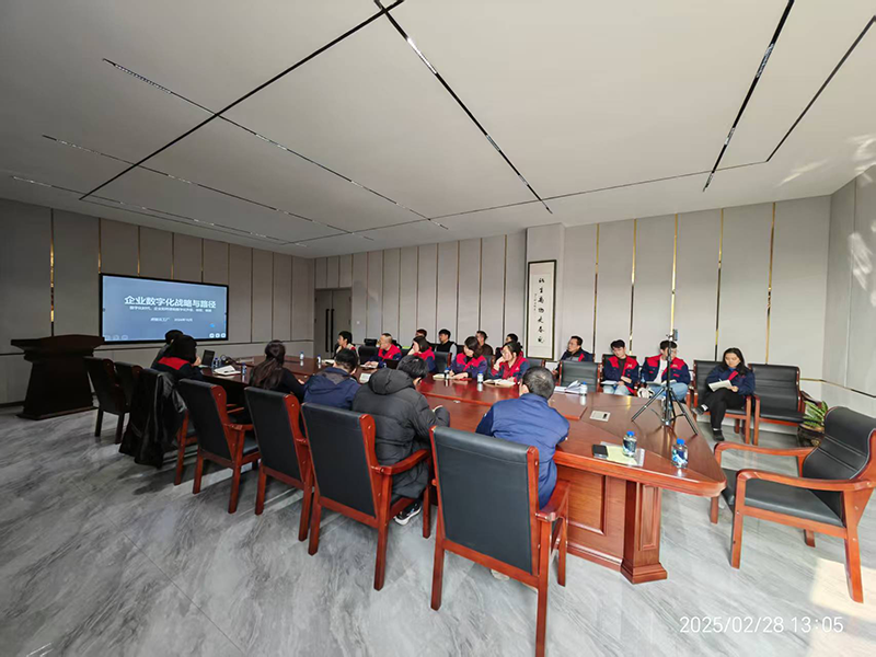
III. Collaborative Innovation Ecosystem
The workstation has assembled a 12-member expert team led by Prof. Li Jianguo from Shanghai Institute of Ceramics, CAS, spanning interdisciplinary fields. Innovative mechanisms feature:
Open innovation challenges: 3 research grants at ¥2 million each
Talent cultivation: Joint "Elite Engineer Program" with NEU to train 30 professionals annually
Technology transfer: Implement "Lab-Pilot-Mass Production" three-stage acceleration system aiming at 40% R&D cycle reduction
IV. Industrial Development Outlook
At full capacity, the silicon carbide project is expected to produce 5,000 sets of semiconductor-grade silicon carbide wafer boats annually, achieving import substitution valued at ¥1.2 billion. Technical specifications will benchmark international leaders like CoorsTek and Kyocera, targeting yield rate improvement from 78% to over 92%. This initiative will catalyze the formation of a local silicon carbide industrial cluster encompassing high-purity powder processing, precision mold manufacturing, and specialty equipment maintenance, creating 300+ employment opportunities.
Related Cases
More >-
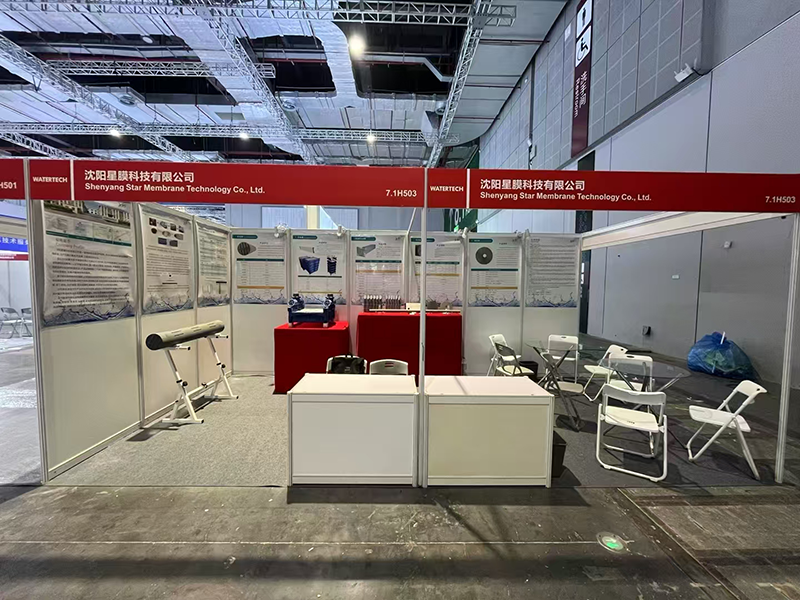
![The 17th Shanghai International Water Exhibition]()
The 17th Shanghai International Water Exhibition
-
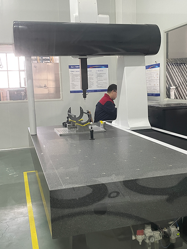
![Three-coordinate detection]()
Three-coordinate detection
-
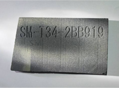
![Machining precision grinding parts]()
Machining precision grinding parts
-
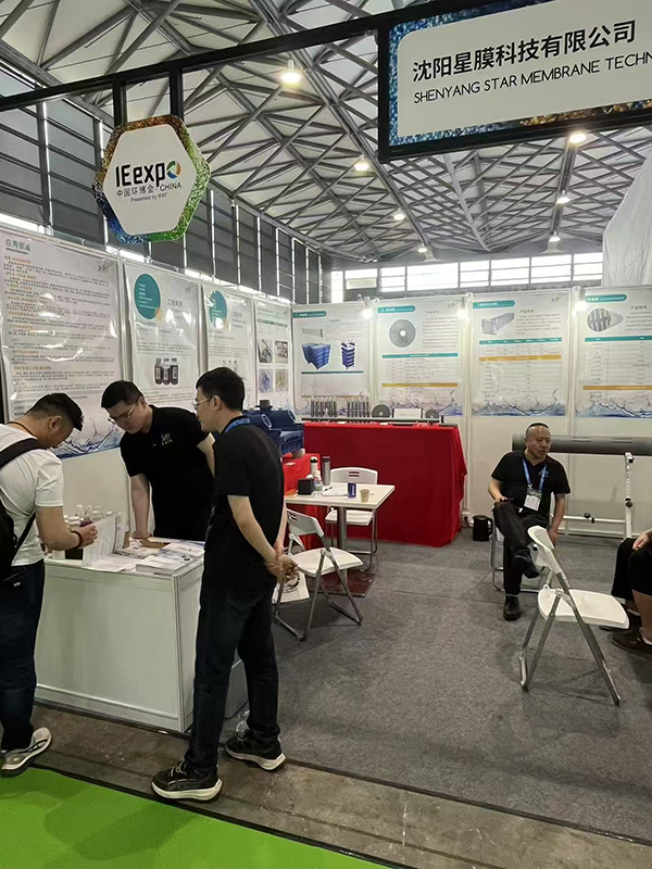
![the 26th IE Expo China in Shanghai]()
the 26th IE Expo China in Shanghai
-
![Application of recrystallized silicon carbide in rotary furnace tube industry]()
Application of recrystallized silicon carbide in rotary furnace tube industry
-
![Production Quality Control Meeting]()
Production Quality Control Meeting
-
![Precision Engineered Silicon Carbide Solutions: Expertise in Manufacturing and Advanced Machining]()
Precision Engineered Silicon Carbide Solutions: Expertise in Manufacturing and Advanced Machining
-
![Transforming Traditional Silicon Carbide Manufacturing into a Digital Factory: Challenges and Opportunities]()
Transforming Traditional Silicon Carbide Manufacturing into a Digital Factory: Challenges and Opportunities
Get the latest price? We'll respond as soon as possible(within 12 hours)