
Technical Training Material: Silicon Carbide (SiC) Properties, Applications, and Industrial Insights
2025-02-28 10:39
1.Introduction to Silicon Carbide
Silicon Carbide, a synthetic compound of silicon and carbon, has emerged as a revolutionary material in advanced manufacturing. First synthesized in 1891 by Edward Acheson, silicon carbide combines exceptional thermal, electrical, and mechanical properties, making it indispensable in high-performance applications ranging from power electronics to aerospace.
2. Key Properties of Silicon Carbide
2.1 Structural and Physical Characteristics
Crystal Structure: Exists in over 250 polytypes (e.g., 3C-SiC, 4H-SiC, 6H-SiC), with 4H-SiC dominating semiconductor applications.
Hardness: Mohs scale rating of 9.5, second only to diamond.
Thermal Conductivity: 120-200 W/m·K, outperforming copper in heat dissipation.
Melting Point: ~2,700°C, suitable for extreme environments.
2.2 Electrical Properties
Wide Bandgap: 3.26 eV (4H-SiC) vs. 1.12 eV for silicon, enabling high-voltage and high-temperature operation.
Breakdown Field: 10x higher than silicon, reducing energy losses.
2.3 Chemical Stability
Resists oxidation, acids, and alkalis up to 1,600°C.

3. Applications of silicon carbide Across Industries
Industry Use Cases:
Semiconductors Power devices (MOSFETs, Schottky diodes), 5G/RF components
Automotive EV inverters:onboard chargers (e.g., Tesla Model 3 SiC traction inverter)
Energy Solar inverters:wind turbine converters, nuclear reactor sensors
Aerospace Satellite components:jet engine thermal coatings
Industrial Cutting tools:abrasives, refractory linings
4.Processing Techniques and Challenges
4.1 Key Manufacturing Steps
Crystal Growth:Sublimation (PVT) for bulk crystals.
CVD for epitaxial layers.
Wafer Processing:Diamond wire slicing, chemo-mechanical polishing.
Device Fabrication:Ion implantation, dry etching.
4.2 Technical Barriers
Wafer Bow: <50 μm curvature required for 150mm wafers.
Yield Rates: ~60% for 200mm SiC epitaxial layers (Q1 2025 industry average).
5.Future Trends in SiC Technology (2025–2030 Outlook)
8-Inch Wafer Adoption: Projected to reduce device costs by 35% by 2028.
Quantum Applications: SiC vacancies for room-temperature quantum computing.
Global Capacity Expansion: China’s SiC production to reach 40% market share by 2027.
6. Conclusion
Silicon Carbide’s unique properties position it as a cornerstone material for sustainable technologies. Understanding the distinction between high-purity and conventional SiC—and their respective roles in power electronics versus industrial systems—is critical for optimizing design and manufacturing strategies. As the industry advances toward 8-inch wafers and novel applications, continuous learning and process innovation will remain essential.
Related News
More >-
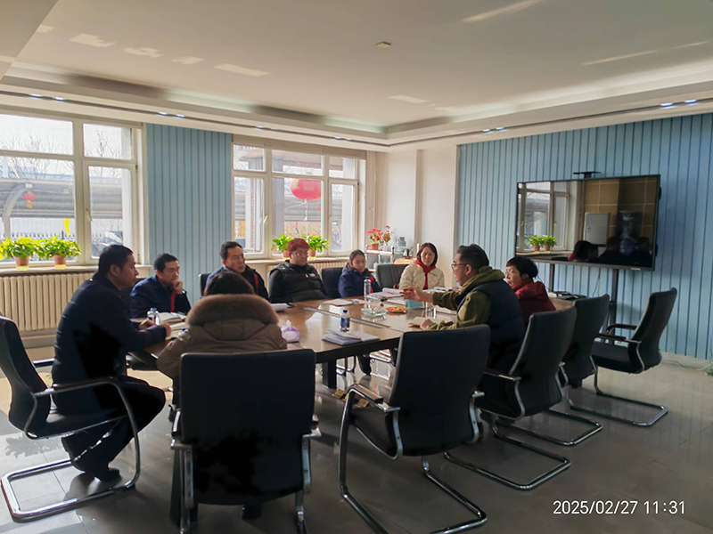
![2025 Sales Plan Discussion Meeting]()
2025 Sales Plan Discussion Meeting
-
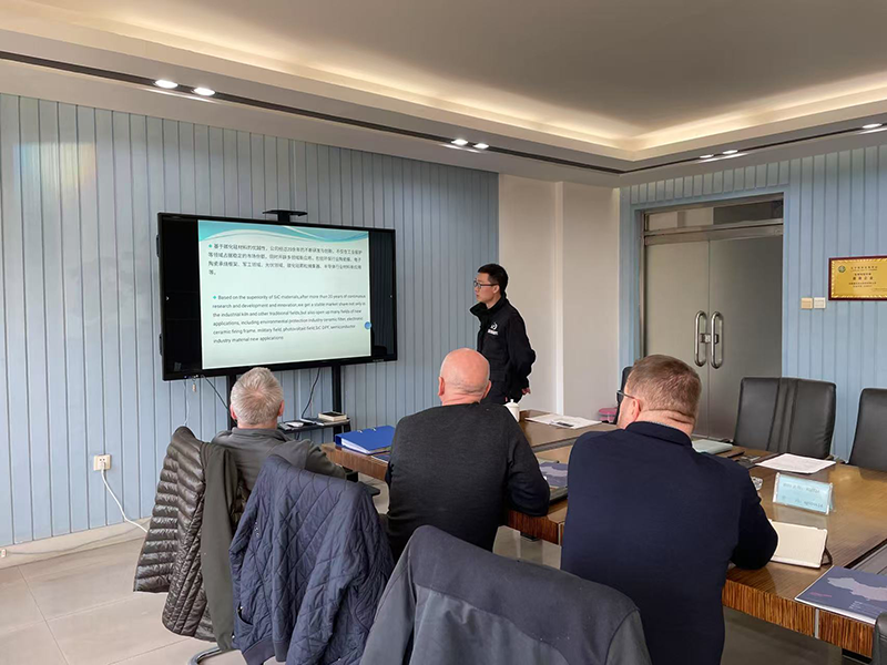
![Germany Customer Visiting]()
Germany Customer Visiting
-
![New Employee Training Sessions]()
New Employee Training Sessions
-
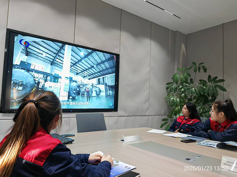
![Semiconductor field customers visit]()
Semiconductor field customers visit
-
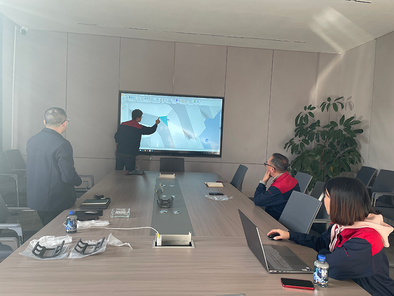
![company study meeting]()
company study meeting
-
![Production Quality Control Meeting]()
Production Quality Control Meeting
-
![The 2024 Liaoning·Shenyang]()
The 2024 Liaoning·Shenyang "Frontier Technology of New Silicon Carbide Materials" Exchange Conference
-
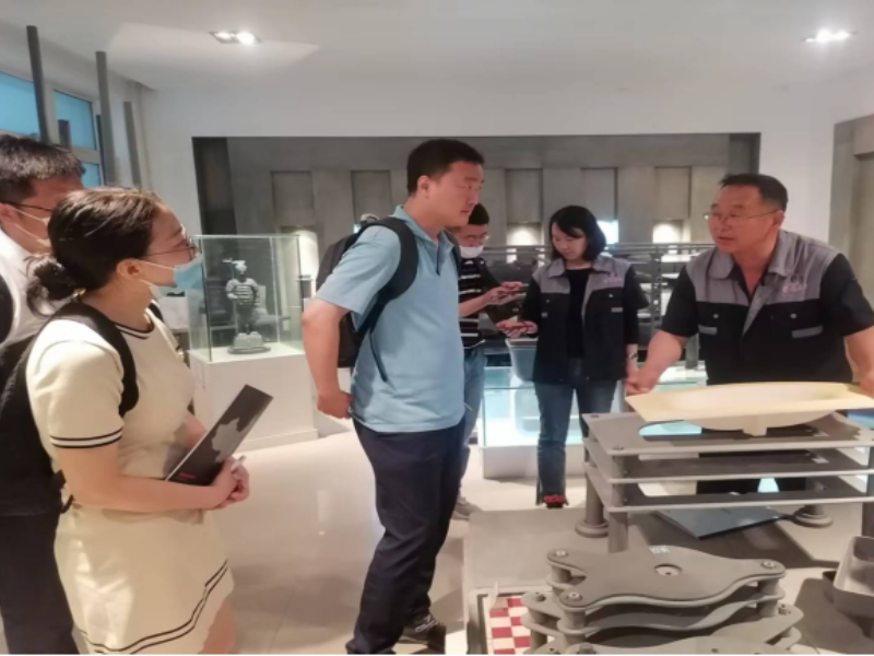
![Industrial Technology Research Institute Supports Starlight Scientific Research And Development]()
Industrial Technology Research Institute Supports Starlight Scientific Research And Development
Shenyang Industrial Technology Research Institute supports Starlight scientific research and development
Get the latest price? We'll respond as soon as possible(within 12 hours)